
![]()
![]()
![]()
![]()
CD Automation represents a reference company for businesses involved in multiple industrial temperature control processes. The Company, active since 1987, produces high-quality thyristor power units, supported internationally by a network of subsidiaries and partners of primary importance in the multi-sector field of thermal regulation.
Through these products, CD Automation reduces complexity and energy consumption and improves the Power Quality of thermal processes, including some manufacturing operations of semiconductor devices.
The value of partnerships
The company’s authority in thermal technologies has facilitated partnerships with other leading players in the sector. In this context, it is particularly interesting to explore the impact of these collaborations in a crucial area for the global market: the production of semiconductor devices.
Since the birth of the first diode, temperature has played a crucial role in semiconductor manufacturing processes. The solutions developed by CD Automation for its partners are based on a deep understanding of the technological processes that form semiconductors. In particular, as the dimensions of these devices have shrunk, temperature has become an increasingly critical variable in the production process.
What is a semiconductor?
The fundamental characteristic of semiconductors is reflected in their name: they are materials whose electrical conductivity lies between that of metallic conductors and insulators. They represent a rather broad and heterogeneous category of substances, highly sensitive to light and characterized by a negative temperature coefficient of electrical resistivity. This means that their conductivity increases as temperature rises, unlike metallic conductors.
The main reason why semiconductors are so useful is that their conductivity can be modified through the addition of impurities (doping), the application of an electric field, or exposure to light.
The semiconductor device crisis
In recent years, the semiconductor sector has experienced a period of strong instability, initially linked to supply chain difficulties that emerged in the post-pandemic period and that particularly affected consumer electronics and the automotive industry. Although the most critical phase of the “chip shortage” has gradually eased, the market continues to be characterized by complex dynamics and highly uneven demand across different application sectors.
From these considerations, it becomes clear that the most accurate term is not simply “chips,” but “dispositivi a semiconduttore”, a term that identifies the entire family of fundamental components of modern electronics (transistors, diodes, and power devices) and which represents the foundation on which industrial electronics has developed and continues to evolve.
How are semiconductor devices manufactured?
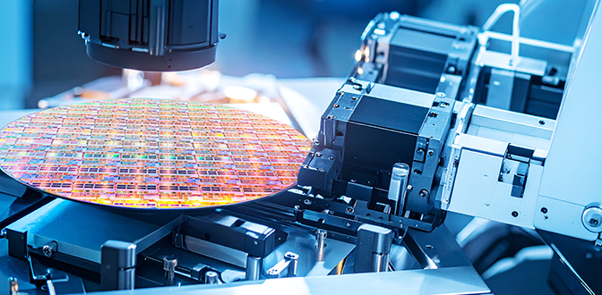
The manufacturing of semiconductor devices refers to the process used to produce the chips and integrated circuits found in most modern electronic devices. This industrial process is carried out through multiple stages involving photolithographic and physicochemical technologies, during which circuits are gradually built on a substrate called a wafer, made from a single crystal of ultra-high-purity semiconductor material.
To create an integrated circuit, an extremely homogeneous wafer is required, free from discontinuities that would compromise component quality. The most widely used semiconductor in the industry is monocrystalline silicon (meaning it has a uniform crystal structure throughout the material), grown using the Czochralski technique.
The Czochralski process
This process consists of the vertical lifting and simultaneous counterclockwise rotation of a properly oriented silicon monocrystalline seed, introduced into molten silicon at 1425°C by means of a metal rod, while the crucible rotates in the opposite direction.
In this way, a small amount of molten material in contact with the seed cools and solidifies according to a crystal structure identical to that of the seed. As the seed is pulled upward, more material solidifies in the same way, producing a single-crystal ingot.
The silicon temperature in the crucible is kept only a few degrees above its melting point, and by adhering to the seed crystal it solidifies very quickly, preserving the seed’s structure. Strict control of the molten material temperature, the chamber atmosphere, the extraction speed, and the complete absence of vibrations allows the production of perfectly cylindrical and highly pure ingots
The float zone method
However, the previously described method has a limitation: silicon tends to react chemically with crucible materials. For this reason, it is preferable to obtain silicon single crystals using the floating-zone technique.
In this case, the ingot is fixed at the upper end to the upper chuck, while its lower part is brought into direct contact with a monocrystalline seed held by the lower chuck. The process begins by creating a molten zone in the part of the ingot in contact with the seed, which is then slowly moved upward. The silicon that solidifies in contact with the seed faithfully replicates its crystal structure.
Defect removal
The next step consists of cutting the ingot using diamond wires to obtain discs a few tenths of a millimeter thick: wafers. The resulting slices have surface imperfections that are removed through a series of processes (grinding and lapping).
The final processing step is chemical etching, which removes the last surface defects, producing monocrystalline wafers ready for component fabrication.
Photolithography
At this stage of semiconductor device manufacturing, complex patterns must be miniaturized and printed onto the wafer through a process known as photolithography.
Initially, the wafer is coated with photosensitive chemicals (photoresist), which harden when exposed to light. A light beam is then projected through a photomask, creating a light image of the circuit. This image is passed through a series of lenses that reduce it to the correct scale and project it onto the wafer.
The light reacts with the photoresist, which is then washed away, revealing an underlying oxide layer. This oxide layer is further etched using acid, exposing the silicon beneath. The exposed silicon is then subjected to a process called doping, which alters its electrical properties.
This process is repeated multiple times, with different combinations of chemicals and masks, until the semiconductor devices are built layer by layer.
Property enhancement
Some layers are baked, others are blasted with ionized plasma, and others are immersed in metals. Each treatment modifies the properties of that layer and gradually forms part of the puzzle that makes up the chip design. Finished silicon wafers contain billions of circuit elements and thousands of individual microchips.
Semiconductor device manufacturing: a continuously evolving sector
A full understanding of these semiconductor manufacturing processes is essential to face the many challenges of a rapidly growing sector that is deeply involved in the evolution of thermal technologies. It is precisely with this goal in mind that CD Automation provides its know-how and offers a family of universal power controllers for semiconductor device production.
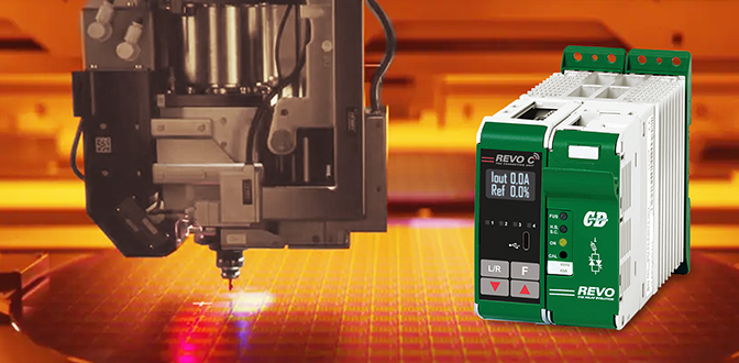
The characteristics of REVO C
REVO C, in the 30 to 2100 A range, is a high-performance power controller for power regulation, adaptable to all SCR applications and equipped with an advanced microprocessor that makes it universal and fully software-configurable.
It is also one of the most complete units in the range thanks to:
- three-phase synchronization, phase rotation diagnostics, phase-angle firing, current limiting, and high measurement accuracy;
- integrated Profinet communication and reduced integration times thanks to TIA Portal libraries; Ethernet/IP communication with dedicated libraries to simplify integration;
- SCCR 100 kA – 600 V (Short Circuit Current Rating) certification, in compliance with UL508 standard.
The main advantage of the REVO C power controller – which makes it particularly suitable for semiconductor device production – is its ability to connect easily with the external world via Bluetooth and the most widely used industrial Fieldbus protocols. Its versatility allows configuration of inputs, firing modes, and control logic directly from a smartphone or personal computer.
Designed and built as a single compact unit, REVO C not only reduces the overall footprint and the time required for assembly and wiring of separate fuses, but also ensures proper execution of testing phases and easy access to printed circuit boards, fuses, and thyristors.
Do you need suggestions to make your thermal control processes in semiconductor manufacturing more efficient and competitive? Contact us and book a free consultation session with one of our experts. You will receive strategic proposals to enhance and extend the lifetime of your heating systems while minimizing downtime.


